 Image 1 of 3
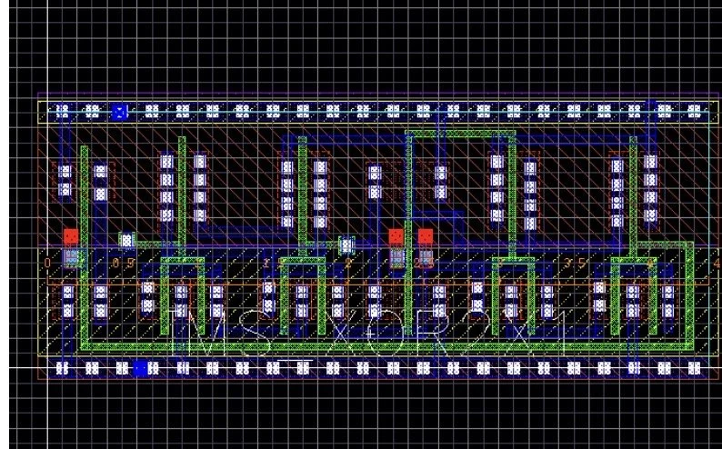 Image 2 of 3
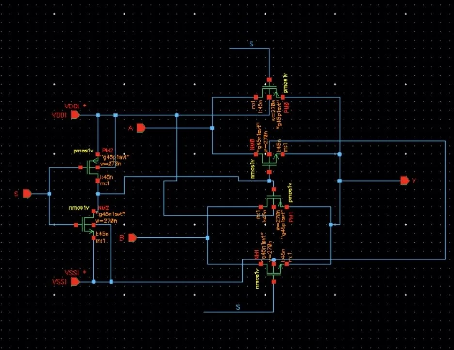 Image 3 of 3
CMOS Digital Circuit Design — Transistor Level Gates
Digital Design Systems — Project 1
Standard cell design often assumes pre-built primitives — this project required building from scratch. I designed and laid out seven CMOS base cells in Cadence Virtuoso at 270nm, including INVX1, INVX4, NAND2, NOR2, XOR2, AOI22, and TMUX2. Each cell was verified for DRC and LVS compliance, with timing analysis performed using ADEXL to characterize rise and fall propagation delays across all input paths.
CMOS Hierarchical Design — Boundary Scan Array
Digital Design Systems — Project 2
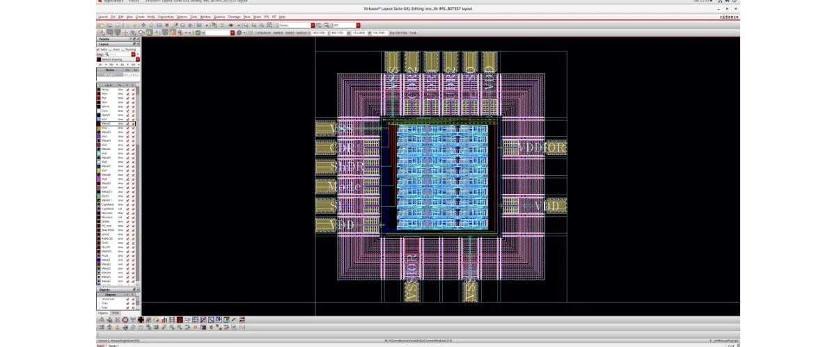
Built a complete boundary scan test architecture hierarchically from the base cells designed in Project 1. Implemented a D flip-flop, full adder, 16-bit adder, and boundary scan cell, scaling up to a 50-register boundary scan chain fitted within a 396×396μm quarter-pad frame. All cells optimized for minimum area and verified DRC and LVS clean.
RTL Design and Verification — DTMF Receiver
Digital Design Systems — Project 3
I designed a memory bus arbiter in Verilog using a REQUEST/GRANT state machine with priority logic, verified through RTL and gate-level netlist simulation including intentional fault injection. Integrated the arbiter into a full DTMF receiver RTL database, performed logic synthesis, DFT test insertion, and timing analysis. Wrote and verified a TDSP assembly language program cross-validated against equivalent C code.
CMOS Digital Circuit Design — Transistor Level Gates
Digital Design Systems — Project 1
Standard cell design often assumes pre-built primitives — this project required building from scratch. I designed and laid out seven CMOS base cells in Cadence Virtuoso at 270nm, including INVX1, INVX4, NAND2, NOR2, XOR2, AOI22, and TMUX2. Each cell was verified for DRC and LVS compliance, with timing analysis performed using ADEXL to characterize rise and fall propagation delays across all input paths.
CMOS Hierarchical Design — Boundary Scan Array
Digital Design Systems — Project 2
Built a complete boundary scan test architecture hierarchically from the base cells designed in Project 1. Implemented a D flip-flop, full adder, 16-bit adder, and boundary scan cell, scaling up to a 50-register boundary scan chain fitted within a 396×396μm quarter-pad frame. All cells optimized for minimum area and verified DRC and LVS clean.
RTL Design and Verification — DTMF Receiver
Digital Design Systems — Project 3
I designed a memory bus arbiter in Verilog using a REQUEST/GRANT state machine with priority logic, verified through RTL and gate-level netlist simulation including intentional fault injection. Integrated the arbiter into a full DTMF receiver RTL database, performed logic synthesis, DFT test insertion, and timing analysis. Wrote and verified a TDSP assembly language program cross-validated against equivalent C code.